Optical Analysis of Photonic-Crystal VCSEL
Analyzed Structure
All the previous tutorials dealt with two-dimensional geometry. Here we will define a three-dimensional structure and perform its optical analysis. This tutorial is base on the article ‘Numerical Methods for modeling Photonic-Crystal VCSELs’ [Dems-2010], which compares several advanced method for analysis of a PC-VCSEL.
Photonic crystal etched in the VCSEL structure breaks its axial symmetry, and, hence, the two-dimensional cylindirical approximation cannot be used any more. Furthermore, strong refractive index contrast between semiconductor layers and photonic crystal pattern causes strong light scattering and a typical linear polarization (LP) approximation is no longer valid. In consequence, application of popular simplified models is impossible, especially in situations where one needs to determine not only the resonant wavelength of the PC-VCSEL cavity, but also the cavity Q-factor or the gain characteristics of the laser.

Schematic structure of PC-VCSEL modelled in tutorial5.xpl file.
The structure for this tutorial is a gallium arsenide PC-VCSEL presented in the figure schematic structure of PC-VCSEL. It consists of single-wavelength long GaAs cavity, sandwiched by 24/29 pairs of top/bottom GaAs/AlGaAs distributed Bragg reflectors (DBRs). The optical gain is provided by three layers of 8 nm-thick InGaAs quantum wells separated by 5 nm GaAs barriers and located together in the anti-node position. The diameter of the optical gain region is set to be the same as the photonic crystal pitch Λ. Details for layer thickness and refractive index values can be found in the table below:
Layer |
Thickness (nm) |
Refractive index |
|
|---|---|---|---|
Top DBR 24 pairs |
69.40 79.55 |
3.53 3.08 |
|
Cavity |
121.71 |
3.53 |
|
Multi quantum wells |
3×8.00 / 2×5.00 |
3.56 / 3.35 |
|
121.71 |
3.53 |
||
Bottom DBR 29 pairs |
79.55 69.40 |
3.08 3.53 |
|
Substrate |
infinite |
3.53 |
|
In the quantum wells the imaginary part of the refractive index is ng for r ≤ Λ and –0.01 for r > Λ.
The photonic crystal is etched in the structure and consists of three rings of a triangular lattice with one missing hole in the center. In the analysis the holes are etched from the top edge of the laser structure down to the specified number of DBR pairs.
Epitaxial layers
Defining epitaxial layers is very similar to the previous tutorials. However, this time we operate in 3D, which means we will have slightly different geometrical objects and we will need to specify three coordinates or dimensions instead of two.
Before you begin defining the geometry, open new PLaSK window and switch to the Defines tab, and define the following parameters:
Name |
Value |
|---|---|
L |
4.0 |
aprt |
L |
d |
0.5 |
totalx |
(6.1*sqrt(3)/2+d)*L |
totaly |
(6.1+d)*L |
etched |
24 |
We will use these values in our geometry. Their meaning is as follows: L is the photonic crystal pitch, R is the radius of the gain aperture, d is the relative diameter of etched holes, totalx and totaly are dimensions of the whole computational region, and etched is the number of etched DBR pairs.
Next, switch to the Materials tab and add three materials. For each of them add property Nr in the right table and set the materials names and Nr values as follows:
Material |
|
|---|---|
GaAs |
3.53 |
AlGaAs |
3.08 |
QW |
3.56 - 0.01j |
Now you may switch back to the Geometry tab. Press  and select
 Cartesian3D from the list. It will create three-dimensional geometry (cartesian3d). In the bottom left of the window, set a name main for the geometry, and type GaAs in the ‘Bottom’ field of the Border Settings (bottom-left one). Next, press again, select Item submenu and choose Stack. Select the new stack in the geometry tree and add another stack. Set its name to bottom-dbr and ‘Repeat’ value to 29. Inside add a Cuboid object, set its ‘Size’ to {totalx} × {totaly} × 0.06940 and the material to GaAs. Now, right-click on the Cuboid node in the geometry tree and select Duplicate from the pop-up menu. You can notice that a copy of the cuboid appeared just above the first one. Select it and change the last Size value (height) to 0.07955 and the material to AlGaAs. Now you should see the multi-layered DBR stack (you may need to select the geometry and click  above the preview area).
Having the bottom DBR defined, we need to add top DBR and the cavity. The simples way to create the top DBR stack is to clone the bottom one (use righ-click menu, or press  on the toolbar). However, if you do it, you will notice that the order of the layers in the top DBR is wrong (GaAs layer should be on top): select the GaAs layer and press
  button on the toolbar, to correct it. Next, select the top DBR stack, set its name to
 top-dbr and change the ‘Repeat’ value to 24.
We need to add another stack for a cavity. Select the topmost stack, press to add another Stack. Next, press  to locate the cavity stack (empty for now) between the DBRs. Now add cavity layers according to the table above.
When adding the quantum well layers, we need to define the gain aperture. Do to this, we first add the Align container and specify default item position as ‘Longitudinal’ center at 0, ‘Transverse’ center at 0, and ‘Vertical’ bottom at 0. In this container, we can place objects one over another and the objects lower in the tree overwrite the previous one. Hence, inside the Align, we add a cuboid of size {totalx}×{totaly}×0.00800 and material QW and next we add a cylinder of ‘Radius’ {R} and ‘Height’ 0.00800. For the cylinder set the material QW and in the ‘Roles’ type gain. This way you have added a uniuform layer of the QW material, but the gain will be specified only inside the cylinder. Because you need to set such regions three times, you can add a name qw to the Align container and use [Repeat object] twice more in the cavity.
When you finish defining all the layers, press F4 and check if the source code of your geometry specification looks similar to the following:
<cartesian3d name="main" axes="x,y,z" back="mirror" front="extend"
             left="mirror" right="extend" bottom="GaAs">
  <stack>
    <stack name="top-dbr" repeat="24">
      <cuboid material="GaAs" dx="{totalx}" dy="{totaly}" dz="0.06940"/>
      <cuboid material="AlGaAs" dx="{totalx}" dy="{totaly}" dz="0.07955"/>
    </stack>
    <stack name="cavity">
      <cuboid material="GaAs" dx="{totalx}" dy="{totaly}" dz="0.12171"/>
      <align name="qw" xcenter="0" ycenter="0" bottom="0">
        <cuboid material="QW" dx="{totalx}" dy="{totaly}" dz="0.00800"/>
        <cylinder name="gain" role="gain" material="QW" radius="{R}"
                  height="0.00800"/>
      </align>
       <cuboid name="interface" material="GaAs" dx="{totalx}" dy="{totaly}"
               dz="0.00500"/>
      <again ref="qw"/>
      <cuboid material="GaAs" dx="{totalx}" dy="{totaly}" dz="0.00500"/>
      <again ref="qw"/>
      <cuboid material="GaAs" dx="{totalx}" dy="{totaly}" dz="0.12171"/>
    </stack>
    <stack name="bottom-dbr" repeat="29">
      <cuboid material="AlGaAs" dx="{totalx}" dy="{totaly}" dz="0.07955"/>
      <cuboid material="GaAs" dx="{totalx}" dy="{totaly}" dz="0.06940"/>
    </stack>
  </stack>
</cartesian3d>
In the code above, we have added a name interface to one of the barriers in the cavity, as it will be helpful later when we define an optical solver.
Photonic crystal
At this point we have defined a simple VCSEL structure with a limited active region and no optical confinement. Now we need to add a photonic crytal. We simulate etching air holes in the structure by overlaying air cylinders over the top DBRs. To do so, right-click on the first Stack in the geometry tree view (the one containing the whole structure). From the pop-up menu select Insert into and then Align. This will create an another container around the stack. Select it and specify Default Items’ Positions as follows:
Longitudinal: |
center |
|
Transverse: |
center |
|
Vertical: |
top |
|
This way bot our VCSEL and photonic crystal lattice will be centered horizontally around 0 and vertically the 0 coordinate will be located near one of the quantum wells.
Now add a Lattice item as a second element of the Align container. Make sure the lattice appears below the VCSEL stack. Lattice is a special container that can contain only one element and it distributes its multiple copies over a regular lattice. To make a photonic crystal, we first need to create a hole to be distributed. Using the same procedure as with other containers, add a cylinder to the lattice. Set its solid material to “air”, radius to “{0.5*d*L}” and the height to “{0.14895*etched}”. Variables L, d, and etched are already defined in the Defines section and mean the photonic crystal pitch, relative hole diameter, and number of the etched DBR pairs, respectively.
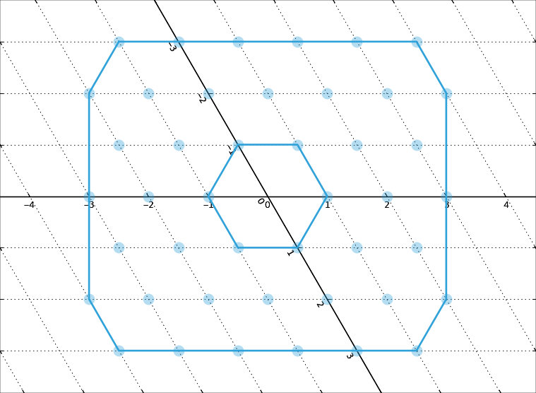
After adding the cylinder, the photonic crysal is still not visible in the preview. Select the Lattice item again and specify Lattice vectors components:
Vector |
Logitudinal |
Transverse |
Vertical |
|---|---|---|---|
First: |
|
|
|
Second: |
|
|
|
This will make triangular lattice. The last thing to do is to specify the lattice boundaries. To to this, click the Edit... button below the Lattice Boundaries* sections. The visual editor opens. By clicking the lattice nodes draw two polygons as in the following figure.
Once you click Ok on the editor, the lattice is completed. You should see the vertical lines in the top DBR region indicating the edges of the holes. You can cat a better preview, by selecting x-y plane in the geometry preview toolbar and by clicking  next to it, to set equal ratio for both axes. You should see a regular lattice of photonic crystal holes.
The last thing to do is cutting only one forth of the geometry. As the main geometry has its left and back edge symmetric, we must clip the geometry to the front-right quarter. To do this, right-click the topmost Align object (the one containing bot VCSEL and the photonic crystal lattice), choose Insert into, and select a Clip object. In the Clipping Box settings set Left and Back to 0. You should see your structure being clipped in the preview. Don’t worry: PLaSK will automatically create the mirror reflections.
Optical Solver
M. Dems, I.-S. Chung, P. Nyakas, S. Bischoff, K. Panajotov, ‘Numerical Methods for Modeling Photonic-Crystal VCSELs,’ Opt. Express 18 (2010), pp. 16042-16054